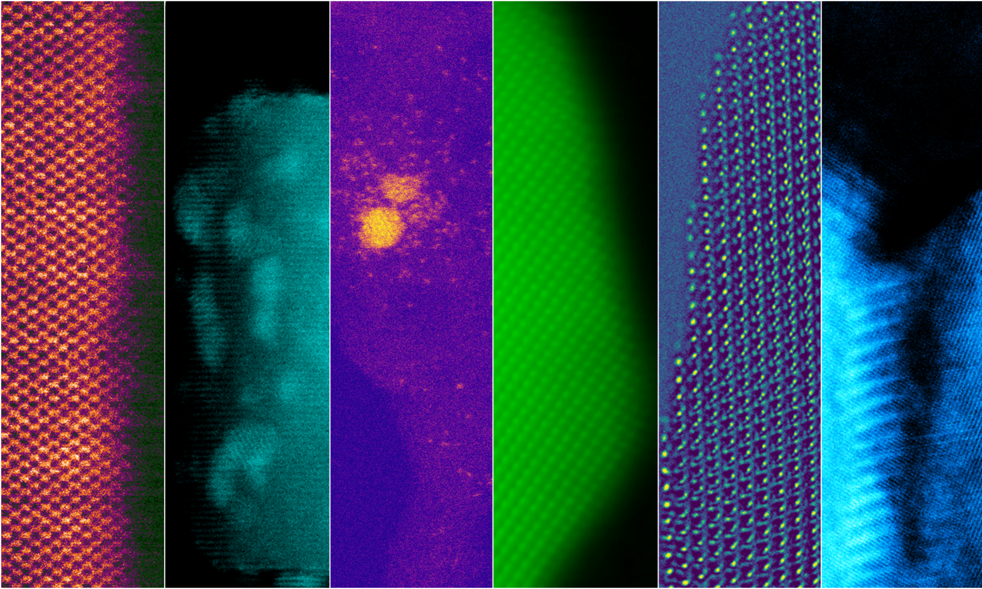
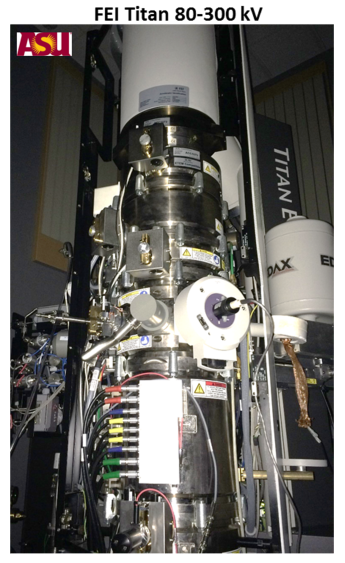
Arizona State University has a world class facility for transmission electron microscopy (TEM). We have a unique set of state-of-the-art, cutting edge instruments which are employed for advanced materials research. The microscopes are housed in the LeRoy Eyring Center for Solid State Science. TEM is a powerful technique for characterizing the nanostructure and nanochemistry of materials. Modern instruments have spatial resolutions of better than 0.1 nm and are capable of providing direct information on bulk, defect and surface structures. This has become an essential tool in determining the structure, composition and bonding in nanomaterials, and it is now critical in fundamental materials research. There are a variety of different imaging, spectroscopic and diffraction techniques available in an electron microscope. Imaging techniques such as phase contrast imaging and Z-contrast imaging can provide atomic structure, defect distribution, strain information and particle and grain morphology. Spectroscopic techniques provide nanoscale composition, electronic bonding information and optical properties. Diffraction techniques can provide structure and crystal symmetry information in addition to localized strain measurements.
Scanning transmission electron microscopy (STEM) focuses the electron beam to subnanometer dimension and is particularly powerful at probing chemical composition with atomic resolution via nanospectroscopy. In energy dispersive x-ray spectroscopy, the incident high energy electron excites atoms in the sample and when these atoms de-excite they may emit an x-ray. The energy of the emitted x-rays is a finger print of the elements present in the material. The excited volume of materials is controlled by the size of the focused electron probe. In a second technique called electron energy-loss spectroscopy (EELS), the incident electron loses energy when it passes through the sample due to interaction with the atoms in the material. The distribution of energy losses contains detailed information on the elemental composition and electronic bonding in the materials. Because the electron beam diameter may be a small as 0.1 nm, this compositional and bonding information is obtained with atomic resolution.
Links to subtopics