I joined the Crozier research group in August 2015 to begin my Ph.D. following my graduation from the University of Arizona with a B.S. in Materials Science & Engineering. My primary driving force for pursing a doctoral degree has always been my fascination with the capabilities of transmission electron microscopy and spectroscopy. From my 4+ years of graduate research, I’ve realized the importance of connecting macroscale functionality with nanoscale defects in materials systems for developing rational design principals.
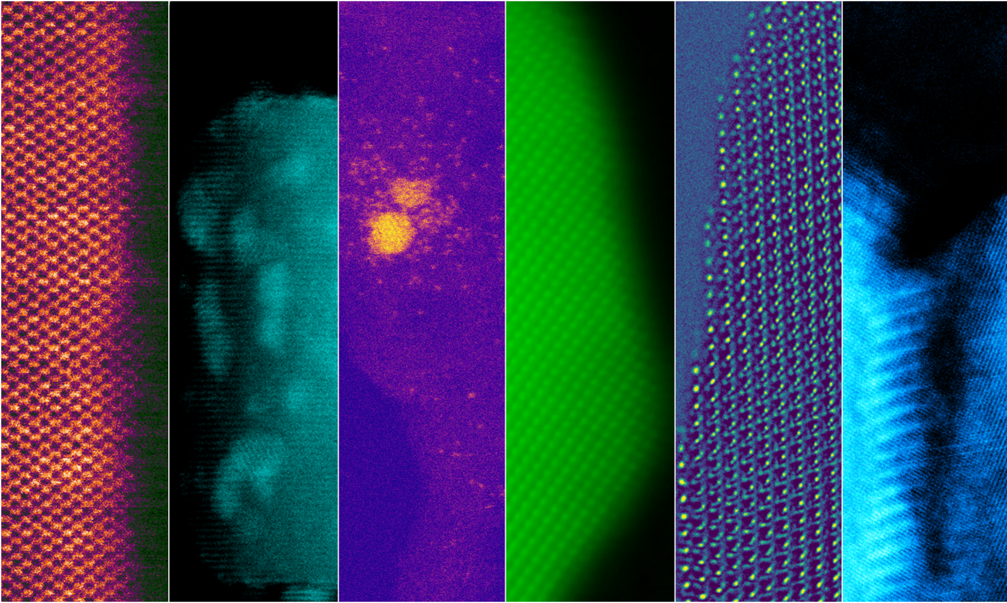
My current research is focused on applying advanced electron microscopy/spectroscopy to understand photocatalyst nanoparticles used for solar fuel production at multiple length scales. Within this topic, I’m focused on two promising materials systems: Pt-functionalized graphitic carbon nitrides and titania-supported ceria. So far, my work has resulted in a new approach for detecting critical defects and disorder in graphitic carbon nitrides. By combining bulk and nanoscale characterization techniques, I can identify the root-cause for reduced performance in these systems allowing design strategies to be addressed.
Outside the lab, I’m involved in undergraduate student mentoring and graduate student professional development. As a founding member and chair for professional development for the Materials Science Graduate Student Community at ASU, I organized a seminar series titled “Excelling Beyond the Lab” that took place throughout the Fall 2018 semester. I’ve also volunteered as an Innovation Associate, and more recently an Academic Associate (a more involved role), for the Engineering Projects in Community Service program at ASU. Through the Fulton Undergraduate Research Initiative, I was able to mentor two undergraduate students (Tu-Uyen Phan and Alex Bravenec) who conducted independent research projects under my supervision.
In my free time I enjoy Melbourne shuffling, playing with my French bulldog, listening to podcasts, and attending music festivals with my friends.
Starting in January 2020, I will be joining Intel as an Packaging R&D Engineer! I am looking forward to utilizing many of the transferable skills I obtained throughout grad school and shifting into a new area of expertise.
Find me online: LinkedIn | Google Scholar
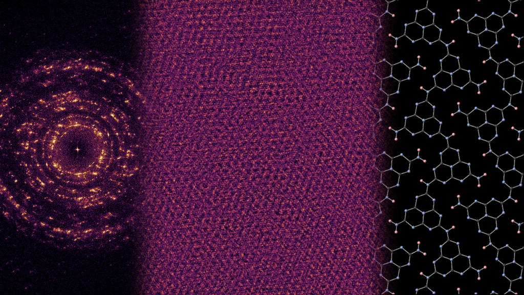
Middle: high resolution TEM image taken with a low electron dose rate, which allows us to directly image the sensitive polymer structure.
Left: a Fourier transform of the image (middle) shows the periodic in-plane structural information.
Right: structure model for perfect, defect-free graphitic carbon nitride.
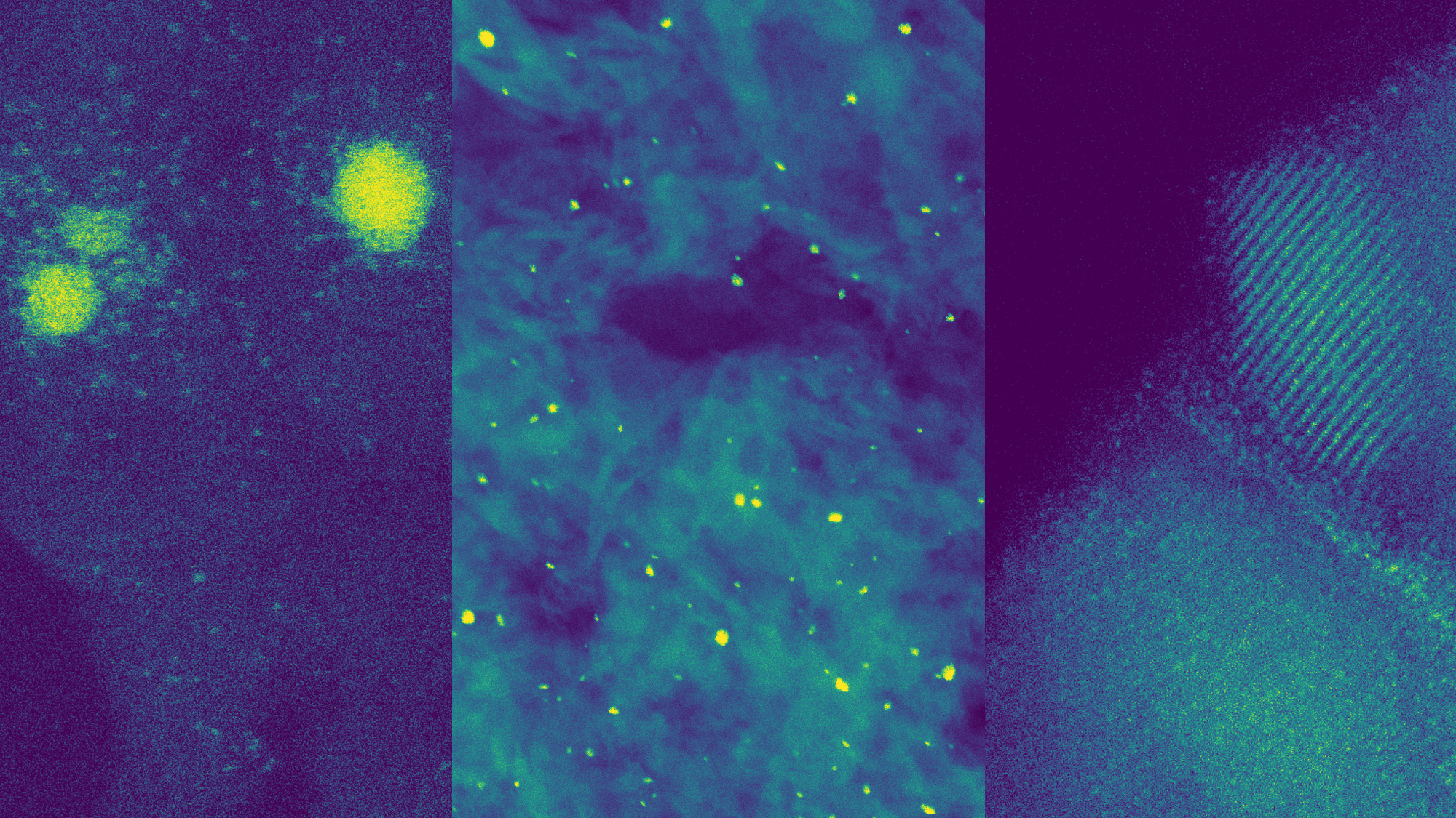
Left and middle: Pt single atoms (left) and nanoparticles (middle) deposited on graphitic carbon nitride supports.
Right: CeO2 and Ce single atoms dispersed on TiO2 anatase particles.